
Google Reportedly Turns to AMD for a Radically Different Kind of AI Chip
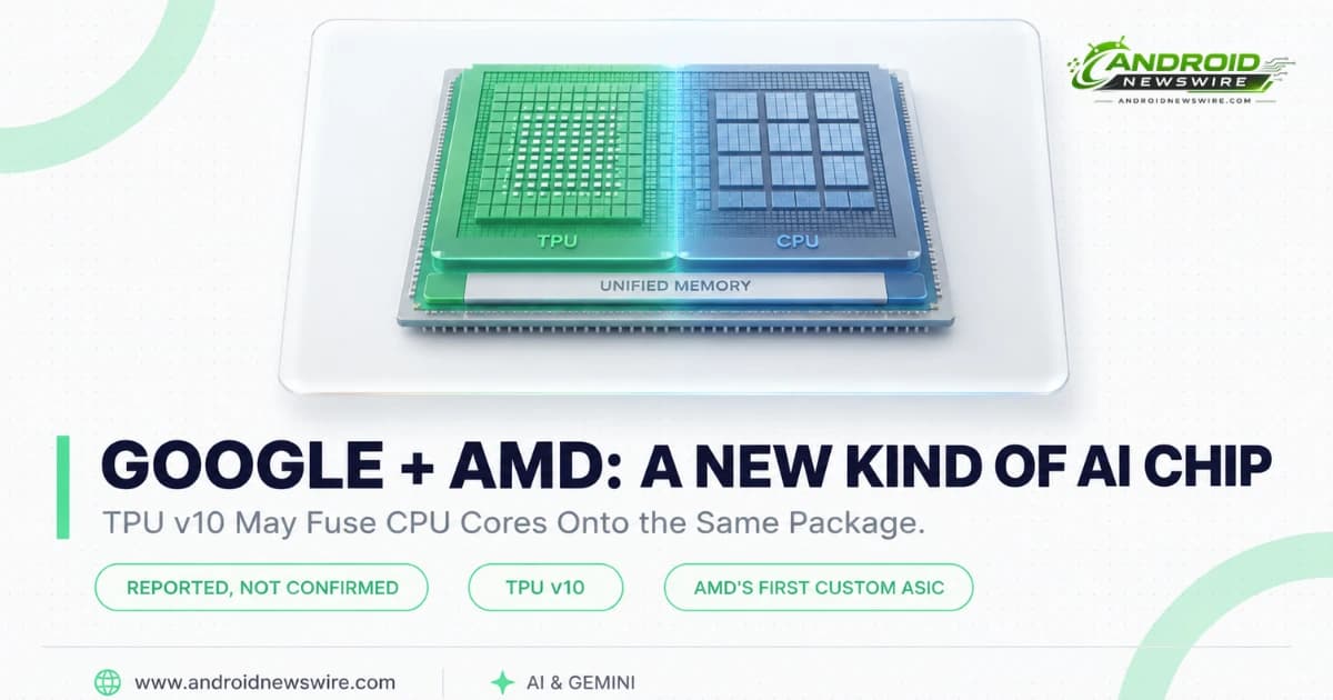
For nine straight generations, Google built its custom AI accelerators – the Tensor Processing Units, or TPUs, that power everything from Gemini training to Google Cloud’s AI infrastructure – with Broadcom as its primary silicon design partner. According to a growing body of industry reporting, that pattern may be about to change in a genuinely unusual way. Google is reportedly working with AMD on its 10th-generation TPU, and the reason for the partnership isn’t simply cost or manufacturing capacity – it’s architectural. Google wants something AMD has already built and nobody else in the industry currently ships at scale: a chip that puts general-purpose CPU cores directly on the same silicon package as an AI accelerator.
What’s Actually Being Reported
The core detail across multiple independent reports is consistent: Google is exploring a hybrid AI accelerator design for its TPU v10 generation that would integrate CPU cores directly into the TPU’s processor package, rather than relying on a separate, physically distinct CPU communicating with the accelerator over a standard interconnect. The stated purpose isn’t general AI training – it’s specifically aimed at reinforcement learning and agentic AI workloads, categories of AI compute that increasingly require tighter, faster interaction between conventional processing and AI acceleration than earlier generations of pure-accelerator chips were built to handle.
It’s worth being precise about the sourcing here, since this is very much a reported story rather than a confirmed one. The detail trail traces back to market chatter from semiconductor research firm SemiAnalysis, further amplified through reporting from Tom’s Hardware and picked up widely from there. Neither Google nor AMD has confirmed the partnership.
Why AMD Specifically – and Why This Is Genuinely Unusual
This is the part of the story that separates it from a routine “company X might work with company Y” rumor. According to Wedbush’s analysis of the reporting, AMD is currently the only vendor shipping a high-volume data center processor that combines x86 CPU cores and GPU chiplets on a single package sharing one unified memory pool – and that specific kind of integration is reportedly exactly what Google’s 10th-generation TPU project needs. AMD’s Instinct MI300A is the concrete precedent here: a real, shipping product that packages Zen CPU cores and CDNA GPU compute resources together inside one unified accelerator package.
That’s a meaningful detail, because it means Google isn’t simply shopping around for a cheaper or faster chip designer – it’s reportedly targeting AMD specifically because AMD has already solved a hard packaging and architecture problem that Google, for all its deep internal AI accelerator expertise, hasn’t built for itself. One report frames the likely rationale directly: Google is said to want help with pieces of the design it isn’t as strong at but AMD excels in, potentially including CPU intellectual property and programming logic that would take Google considerably longer to develop independently.
This Doesn’t Replace Broadcom – It’s a Parallel Track
A detail worth stating clearly, since it’s easy to misread this as Google abandoning its existing chip partner: Google’s relationship with Broadcom, which covers conventional TPU design and manufacturing, reportedly extends through at least 2031, and analysts have specifically noted the AMD collaboration is unlikely to replace that arrangement. The reported AMD-designed hybrid chip appears to be targeting a different category of workload entirely – reinforcement learning and agentic AI specifically – rather than serving as a wholesale replacement for the TPU line Broadcom has helped build across nine generations.
That framing also fits a broader pattern that’s become increasingly visible in Google’s chip strategy over the past year. Google has reportedly already brought MediaTek into its TPU supply chain for its seventh-generation chips, and this week’s separate reporting about Google taking a $12.2 billion stake in Marvell for custom AI chip work adds yet another thread to the same story. Google, in other words, appears to be deliberately diversifying its silicon partnerships across multiple specialized vendors – Broadcom, MediaTek, Marvell, and now potentially AMD – rather than consolidating its custom chip strategy around any single design partner.
What This Would Mean for AMD
If this reporting holds up, the significance for AMD specifically shouldn’t be understated. This would represent AMD’s first real, deep involvement in a custom AI ASIC project for an outside hyperscaler – a genuinely different category of business than AMD’s existing chip lineup, and one industry analysts have flagged as a meaningful new revenue avenue. AMD has built substantial expertise in exactly the kind of hybrid CPU-accelerator packaging this project reportedly requires, but hasn’t previously had a marquee customer relationship of this scale putting that expertise directly to work for someone else’s custom silicon.
The Business Context: A Shrinking TPU Output Forecast
There’s a less flattering data point tucked into this same reporting cycle worth including for full context. Alongside the AMD partnership chatter, SemiAnalysis reportedly flagged lower TPU output expectations for the second half of 2026 than previously forecast, attributed to capacity challenges ramping up advanced chip packaging technology. Google’s seventh-generation TPU (codenamed “Ironwood”) unit projections were reportedly revised down from 3.2 million to 2.7 million units, with Broadcom separately cutting its own 2026 advanced-packaging wafer output targets.
That context matters for how to read the AMD story overall. This isn’t happening against a backdrop of unlimited chip-manufacturing capacity and Google simply adding more partners for convenience – it’s happening while Google’s existing TPU supply chain is reportedly running into real capacity constraints, which arguably strengthens the logic for bringing in additional specialized partners across different parts of the chip design and manufacturing pipeline, rather than depending entirely on any single relationship.
Why This Matters Beyond the Data Center
For anyone following Android and Pixel specifically, it’s worth being clear about scope: TPUs used inside Google’s data centers for AI training and inference are architecturally distinct from the Tensor chips inside Pixel phones, even though both fall under Google’s broader custom-silicon strategy. This reported AMD collaboration is squarely a data-center and cloud infrastructure story, not a direct signal about the next Pixel chip.
That said, it’s a useful data point for understanding just how seriously Google is investing in AI infrastructure at the moment its own competitive position against OpenAI and Anthropic is under real pressure – a theme that’s run through several of Google’s biggest stories this year, from the DeepMind leadership reshuffle to Gemini’s rapid model release cadence. A company willing to bring in a first-time hardware partner specifically to solve a hard architectural problem it can’t easily solve alone is a company treating its AI infrastructure roadmap as genuinely urgent, not routine.